A diode is a two-terminal device that, roughly speaking, conducts electric current in one direction (from anode to cathode, called forward-biased) much better than the opposite direction (reverse-biased). A small positive voltage at the diode’s terminal biases the diode in the forward direction and can produce a large current. A negative voltage biases the diode in the reverse direction and produces little current even at large voltage values.
Forward Characteristics Reverse Characteristics
Different Types of Diode and Their Applications :
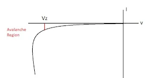
Zener Diode : The Zener diode is always connected as a reverse-biased diode. It is also called as voltage-reference ,voltage-regulator diode. It differs from rectifier diode that it is operated in reverse breakdown region.
Applications : One important application of the Zener diode is in voltage regulation. A voltage regulator is a circuit or device that holds an output voltage constant during output load variations. It is also used as a fixed reference voltage in transistor biasing circuits. As a peak clipper or limiter in waveshaping circuits as it limits one side of a sinusoidal waveform to while limiting the other side to approximately zero,Protection against damage.
The Schottky Diode : A Schottky diode is a junction of a lightly doped -type semiconductor with a metal electrode such as gold , silver , platinum. Thus in Schottky Diode, there is metal to semiconductor junction rather than PN junction. When the diode is forward-biased, the electrons move from the N-type material to the metal and give up their energy quickly. Since there are no minority carriers (holes) the conduction stops quickly and changes to reverse-bias.
Applications : As a switching device in digital computers, As low voltage rectifier because we have to substract only 0.25 V instead 0.7 V , As Schottky TTL logic circuits, To rectify high frequency signals.
The Tunnel Diode : The conventional junction diode uses semiconductor materials that are lightly doped with one impurity atom for ten-million semiconductor atoms. In a tunnel diode the semiconductor materials used in forming a junction are doped to the extent of one-thousand impurity atoms for ten-million semiconductor atoms. This gives rise to the region of negative resistance. Also produces an extremely narrow depletion zone. It have low value of inductance and capacitance.
Application : As tunneling mechanism takes place at the speed of light , it is used as ultra-high speed switching device, As a logic memory storage device, Used in an oscillators and microwave amplifiers.
Varactor Diode : The varactor, or varicap, is a diode that behaves like a variable capacitor, with the PN junction functioning like the dielectric and plates of a common capacitor. A varactor diode uses a PN junction in reverse bias. When reverse bias voltage decreases, the depletion region widens. This increases dielectric thickness which is in turn reduces capacitance. When reverse biars voltage increases , the depletion region narrows down, this increases dielectric thickness which is in turn reduces capacitance.
Application : A voltage controlled capacitance is useful in tuning applications, varactor diode is also used in automatic frequency control device , As adjustable band-pass filter.
Step-Recovery Diode : Step-recovery diode employs a graded doping in which doping level reduced as the junction region approaches. It indicates that less charge carrier density at junction area. This type of doping affects the time required for the device to switch from on stage to off stage and vice-versa. In step-recovery diode, during the negative-half cycle, reverse current exists for short time and suddenly drops to zero. Since reverse recovery period is very sharp, it is called as step-recovery diode.
Application : In frequency multiplier , In ultra-high frequency switching applications.
PIN Diode : PIN diode consists of three semiconductor materials. P type material and N type material is separated by intrinsic material. The intrinsic region offers high resistance to the current flow through PIN diode. The capacitance between the P and N region decreases due to increased separation between N and P regions, it gives fast response time. When a PIN diode is forward biased, it acts like variable resistance. While in reverse biased mode, PIN diode acts as constant capacitance.
Application : As a d.c. controlled microwave switch , As modulator, In attenuater as its resistance can be controlled by the current.
Photodiode : Photodiode is a PN junction device , which operates in a reverse bias. Photodiode differs from a rectifier diode in a sense that its reverse current increases with the light intensity at PN junction. When there is no light incident light , reverse current almost is zero. Resistance of the photodiode is controlled by light intensity. Photodiode can be used to switch on the current at very fast rate.
Application : In Photodetection , In demodulation , In encoders etc.


